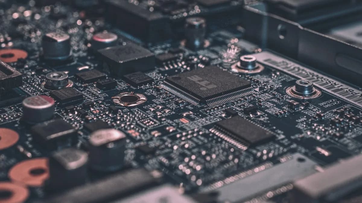
India's Cabinet Committee on Economic Affairs approved the country's first outsourced semiconductor assembly and test plant under the India Semiconductor Mission on Sunday, greenlighting a 4.8 billion dollar facility near Bengaluru operated by Tata Electronics and Taiwan's Powerchip subsidiary PSMC. The plant targets 50,000 wafer starts per month by 2028, focusing on advanced packaging for automotive and smartphone customers.
Minister of Electronics and IT Ashwini Vaishnaw said the approval includes 50 percent capital expenditure support capped at 1.9 billion dollars, matching incentives offered to Micron's Gujarat assembly plant. Karnataka chief minister Siddaramaiah allocated 1,200 acres in Devanahalli adjacent to Kempegowda International Airport for logistics efficiency.
Strategic Rationale
India consumes more than 10 billion dollars in imported chips annually while assembling 1.5 billion smartphones domestically. OSAT capacity reduces re-export of bare dies to Malaysia and Vietnam for packaging, shortening lead times for brands like Apple and Samsung operating Indian factories.
Apple supplier Foxconn welcomed domestic OSAT availability in supplier diversity reviews after 2022 supply-chain shocks. Tata Electronics already supplies mechanical enclosures; packaging integration moves the group up the value chain.
Technology Scope
PSMC will transfer fan-out wafer-level packaging and 2.5D interposer capabilities used in AI accelerator modules. Initial customers include MediaTek chipsets for mid-range phones and Tata's own automotive electronics joint venture with Jaguar Land Rover.
Equipment orders with ASM Pacific Technology and Kulicke & Soffa are scheduled for signing in August. Talent development partnerships with Indian Institute of Science aim to graduate 2,000 packaging engineers by 2027.
Competitive Landscape
Malaysia's OSAT giants ASE and Amkor dominate global share; India's entry pressures pricing in South Asian corridors. U.S. CHIPS Act allies view Indian OSAT as diversification from Taiwan concentration, though leading-edge nodes remain absent domestically.
China's packaging investments in Jiangsu province proceed on larger scale, but export restrictions on advanced AI chips limit overlap in high-end segments India targets for automotive and telecom.
Execution Risks
Land acquisition protests in Karnataka delayed other industrial projects last year; state officials signed community benefit agreements funding vocational schools in four surrounding villages. Water recycling mandates require 80 percent reuse, critical in a region facing monsoon variability.
Investors bid up Tata Group shares 2.1 percent Monday. Vaishnaw said two additional fab proposals — from Tower Semiconductor and a Vedanta-Foxconn consortium — remain under review with decisions expected before Diwali.
The approval marks India's transition from incentive announcements to concrete packaging capacity, a milestone Vaishnaw said will appear in Prime Minister Narendra Modi's Independence Day address if construction begins on schedule in October.
Downstream Manufacturing
Smartphone assemblers in Tamil Nadu and Uttar Pradesh said domestic OSAT capacity could reduce customs delays on re-imported packaged chips by seven to ten days, a meaningful advantage for just-in-time production schedules tied to festival-season demand spikes.
Japan's Ministry of Economy, Trade and Industry hosted a trilateral workshop with Indian and U.S. officials on packaging standards alignment, seeking interoperable quality metrics that simplify multinational customer audits across Arizona, Kumamoto, and Bengaluru sites.
Credence Wire will update this story as officials release revised figures, company filings, or regulatory guidance affecting the developments described above.
GlobalFoundries and STMicroelectronics sent observer teams to Bengaluru planning workshops, evaluating whether India's packaging incentives could complement their own European and Singapore OSAT investments without cannibalizing existing customer allocations.